Custom PCB Design: The Ultimate Guide to Tailored, High-Performance Printed Circuit Boards

In today’s competitive electronics landscape, custom PCB design has become the cornerstone of innovation for engineers, product developers, and OEMs who demand performance, reliability, and cost-efficiency that off-the-shelf solutions simply cannot provide. Whether you are creating a compact IoT sensor, a high-speed communication module, or a rugged WiFi outdoor smart socket that must withstand tropical humidity and temperature extremes, a well-executed custom PCB design ensures your product meets exact electrical, mechanical, thermal, and environmental requirements while optimizing for manufacturability and scalability.
This comprehensive guide explores every critical aspect of custom PCB design — from foundational concepts and detailed development steps to real-world challenges, proven solutions, and practical FAQs. Optimized for those searching for custom PCB design services, custom circuit board design, custom PCB layout, custom PCB schematic design, high-speed custom PCB design, or DFM in custom PCB design, the article draws on industry best practices to help you avoid costly revisions and accelerate time-to-market.
By the end, you’ll understand why thoughtful custom PCB design does more than connect components — it delivers devices that “just work” in the real world, giving your team confidence and your customers lasting value.
What Is Custom PCB Design?
Custom PCB design is the disciplined engineering process of creating a printed circuit board specifically tailored to the unique functional, performance, size, cost, and environmental requirements of a particular product or application. Unlike standard or off-the-shelf PCBs that follow generic specifications, a custom PCB design starts from a clean slate: every trace, via, layer stack-up, component placement, and material choice is optimized for the intended use case.
At its core, custom PCB design encompasses two primary phases:
- Schematic capture — translating the electrical circuit into a logical diagram with components, connections, and netlists.
- PCB layout — physically arranging components, routing traces, defining copper planes, and ensuring signal integrity, power integrity, and manufacturability.
Key elements that distinguish custom PCB design include:
- Precise layer stack-up engineering (symmetric or asymmetric, impedance-controlled)
- High-density routing for fine-pitch components (including BGA, QFN, and micro-BGA packages)
- Controlled impedance for high-speed signals (50 Ω single-ended, 90–100 Ω differential)
- Thermal management features (thermal vias, copper pours, heat sinks)
- Design for Manufacturability (DFM) and Design for Assembly (DFA) integration from day one
- Material selection tailored to application (high-Tg FR-4, Rogers laminates for RF, metal-core for heat dissipation)
In practice, custom PCB design shines in embedded systems and IoT products. For a WiFi outdoor smart socket, custom PCB design might include a 6-layer stack-up with dedicated RF layers for 50 Ω antenna impedance, thermal vias under the relay for efficient heat dissipation, and robust grounding to minimize EMI in a humid outdoor environment.
From a human perspective, excellent custom PCB design means your product performs exactly as intended — reliable, efficient, compact, and durable — without the compromises of generic boards. It represents the perfect fusion of electrical engineering, mechanical constraints, and manufacturing realities that turns innovative ideas into market-ready hardware.
Related terms such as custom circuit board design, bespoke PCB layout, high-density custom PCB design, and impedance-controlled custom PCB design reflect the growing demand for boards that are not just functional but truly optimized.
The Step-by-Step Custom PCB Design Process
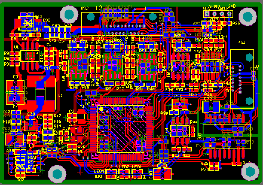
Creating a successful custom PCB design is a structured, iterative process that begins early in the product lifecycle and demands close collaboration between designers, engineers, and fabrication partners. Below is a proven 8-step workflow, illustrated through our WiFi outdoor smart socket example (a rugged IP65 device requiring multilayer construction, controlled impedance WiFi routing, relay power management, and environmental resilience).
1. Requirements Gathering and Feasibility Analysis
Define functional needs (voltage, current, signal speeds, interfaces), non-functional constraints (size, power budget, operating temperature, regulatory compliance), and target production volume. Perform initial cost and manufacturability assessments. For the smart socket, this included specifying 2.4/5 GHz WiFi performance and IP65 environmental rating.
2. Schematic Capture and Circuit Simulation
Create a detailed schematic using tools like Altium Designer, KiCad, or OrCAD. Simulate critical circuits for signal integrity, power integrity, and timing. Add decoupling, filtering, and protection circuitry early.
3. Component Selection and Library Creation
Choose components based on performance, availability, cost, and footprint. Build or verify a complete component library with accurate footprints, 3D models, and simulation parameters.
4. PCB Stack-Up Definition and Layer Planning
Design a symmetric or asymmetric layer stack-up (typically 4–12 layers for IoT applications). Define dielectric thicknesses, copper weights, and reference planes to achieve target impedances and minimize crosstalk. For the smart socket, a 6-layer stack-up was chosen with dedicated ground and power planes.
5. Component Placement and Floor Planning
Strategically place components to minimize trace lengths for high-speed signals, group related functional blocks, and optimize thermal and mechanical layout. Critical components (MCUs, antennas, relays) receive priority placement.
6. Routing and Trace Optimization
Route signals according to design rules: length matching for differential pairs, controlled impedance traces, orthogonal routing on adjacent layers, and short return paths. Use autorouters sparingly and manually optimize critical nets.
7. Design Rule Check (DRC), DFM/DFA Review, and Simulation
Run comprehensive DRC, signal integrity (SI), power integrity (PI), and thermal simulations. Collaborate with your fabrication partner for a formal DFM review to catch issues like minimum trace width, via aspect ratio, solder mask clearance, and panelization.
8. Gerber/ODB++ Output, Documentation, and Release
Generate fabrication and assembly files (Gerber, drill, BOM, PnP, assembly drawings). Include detailed stack-up drawings, impedance notes, and test requirements. Lock the design for production.
This methodical custom PCB design process typically reduces revisions by 50–70% and ensures first-pass manufacturing success when DFM is integrated from the schematic stage.
Common Problems in Custom PCB Design and Proven Solutions
Even experienced teams encounter hurdles in custom PCB design. Here are the most frequent issues and practical, industry-proven solutions:
- Signal Integrity Issues (Reflections, Crosstalk, EMI) Cause: Long traces, improper referencing, or split planes. Solution: Use continuous ground planes, short return paths, and controlled impedance routing. Perform SI simulations early.
- Power Integrity and Ground Bounce Problems Cause: Inadequate decoupling or distant power/ground planes. Solution: Place decoupling capacitors close to IC power pins and use multiple vias for plane connections.
- Thermal Management Challenges Cause: High-power components without adequate heat-spreading paths. Solution: Incorporate thermal vias, copper pours, and symmetric copper distribution; simulate thermal performance.
- Board Warpage or Bowing Cause: Asymmetric stack-up or uneven copper distribution. Solution: Enforce mirror symmetry and copper balancing with thieving patterns.
- DFM Violations Leading to Low Yield Cause: Overly aggressive tolerances or unmanufacturable features. Solution: Run DFM checks with your manufacturer before final release and follow IPC standards.
- Component Placement and Routing Congestion Cause: Poor floor planning in high-density designs. Solution: Group functional blocks and prioritize critical nets during placement.
- Impedance Control Failures Cause: Incorrect dielectric spacing or material variation. Solution: Specify impedance callouts clearly and request test coupons with every fabrication order.
Early DFM collaboration with an experienced partner like TJHXPCB prevents most of these custom PCB design pitfalls.
6 Common Questions About Custom PCB Design (with Clear Answers)
1. What is the main difference between custom PCB design and using off-the-shelf boards?
Custom PCB design creates a board tailored exactly to your electrical, mechanical, and environmental needs, while off-the-shelf boards force design compromises that can limit performance, size, or reliability.
2. How important is DFM in custom PCB design?
Extremely important. Integrating DFM early prevents manufacturing delays, reduces costs, and improves yield. A good fabricator’s DFM review is one of the highest-ROI steps in the process.
3. What tools are best for custom PCB design?
Popular professional tools include Altium Designer, KiCad (free and powerful), Cadence Allegro, and Mentor Graphics. Choose based on team size, complexity, and integration needs.
4. How does custom PCB design impact product cost?
While initial design effort is higher, a well-optimized custom PCB design reduces material costs, improves yield, simplifies assembly, and shortens overall time-to-market — delivering lower total cost of ownership.
5. When should I consider high-speed or RF-specific custom PCB design practices?
Any design with signals above 50 MHz or RF elements (WiFi, Bluetooth, 5G) benefits from controlled impedance, dedicated reference planes, and careful routing practices.
6. What does the future hold for custom PCB design?
Expect wider adoption of AI-assisted routing, embedded component technology, advanced materials for 5G/6G, and tighter integration with simulation and manufacturing data for even faster, more reliable custom boards.
Our Expertise in Custom PCB Design — TJHXPCB, Your Trusted China Partner
At TJHXPCB, custom PCB design is our passion and core competency. As a China-based leader in advanced electronics and IoT solutions, we specialize in delivering fully tailored, high-performance printed circuit boards that meet the most demanding requirements — from rapid prototypes to volume production.
Our custom PCB design capabilities include:
- End-to-end custom PCB design from schematic to Gerber release
- Advanced multilayer (up to 20+ layers), HDI, rigid-flex, and high-frequency designs
- Precise impedance control, thermal management, and signal integrity optimization
- Comprehensive DFM/DFA reviews and SI/PI/thermal simulations
- Seamless integration with turnkey PCB manufacturing and electronic assembly
- Full regulatory and certification support (CE, UL, RoHS, SS standards)
We have successfully executed custom PCB design projects for WiFi outdoor smart sockets and similar rugged IoT products that deliver stable wireless performance, efficient power management, and exceptional durability,As a professional PCB manufacturer based in Tianjin, China, serving global clients including Singapore, Southeast Asia, Europe and North America. Our agile, collaborative process combines state-of-the-art CAD tools with deep engineering expertise — ensuring every custom board is optimized for performance, manufacturability, and long-term reliability.
Whether you need a complete custom PCB design from concept to production, design consultation and optimization, or a full turnkey solution, TJHXPCB delivers faster, more reliably, and more cost-effectively than generic providers.
Ready to bring your innovative idea to life with a superior custom PCB design? Contact our experts today for a free initial consultation, DFM review, and detailed quotation. Let’s co-create the tailored, high-performance circuit boards that power your success.
Reach out via our website or email — your perfect custom PCB design solution awaits.